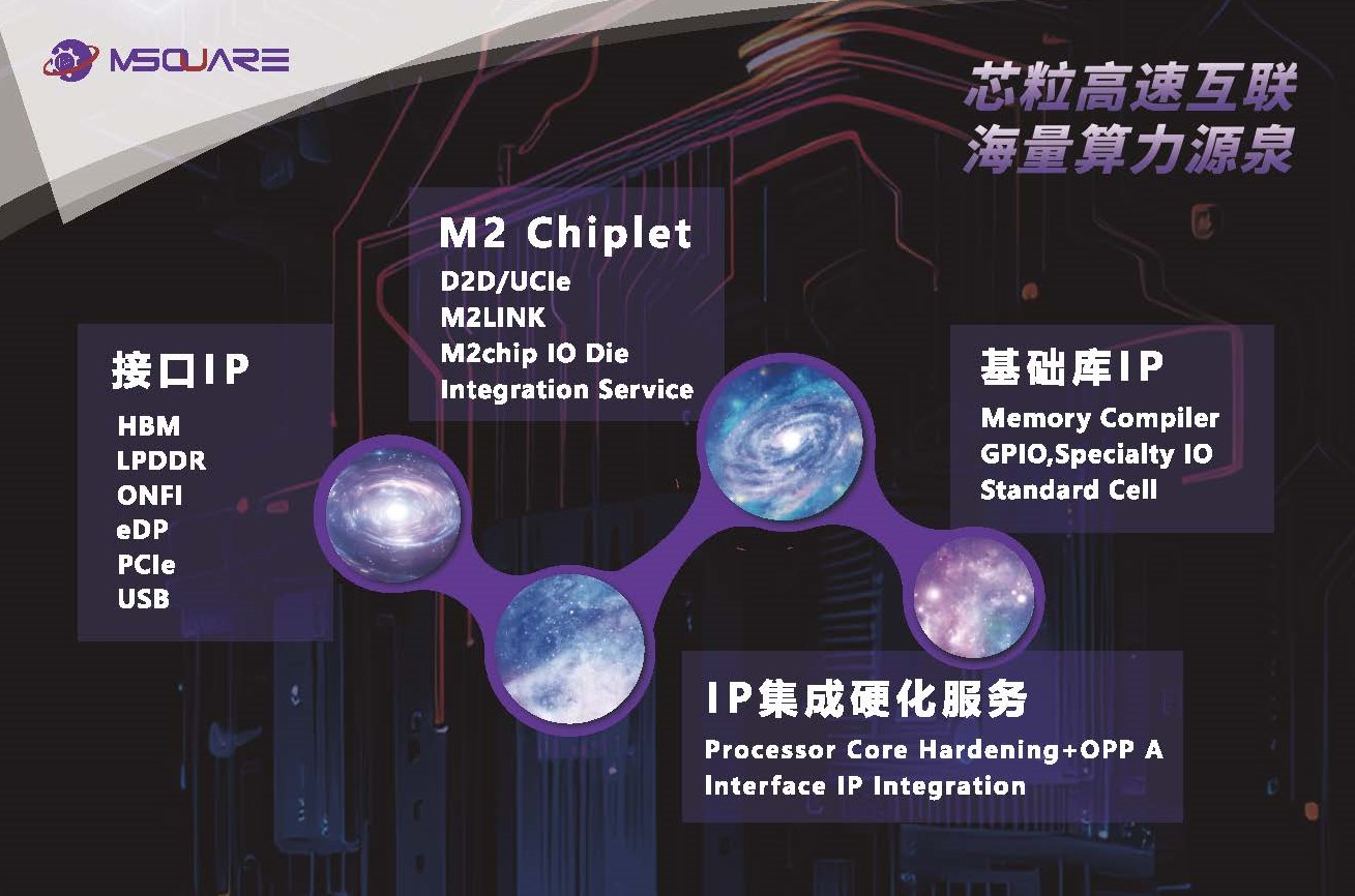

灿芯半导体推出基于中芯国际14nm FinFET工艺的ONFI 4.2 IO和物理层IP
中国上海 - 2021年6月3日 - 定制芯片设计、生产及IP授权的高新技术企业——灿芯半导体日前宣布推出基于中芯国际14nm FinFET工艺的ONFI 4.2 IO及物理层IP,该IO支持SDR/NV-DDR/NV-DDR2 1.8V, NV-DDR3 1.2V, 该物理层IP采用全数字设计,具有低功耗、面积小等特点。

此次推出的ONFI物理层IP可应用于开放式NAND闪存界面,兼容ONFI 4.2/4.1/4.0/3.2等标准,目前该IO及物理层IP已经在中芯国际40nm及14nm FinFET工艺上通过硅验证。
ONFI 4.2物理层IP具有如下特点:
-基于中芯国际14nm FinFET、 40LL工艺,并通过流片验证测试
-支持14nm FinFET NV_DDR3 1.2V Max 1600Mbps; NV_DDR21.8V Max 800Mbps
-支持40LL Max 800Mbps
-支持芯片内终端匹配电阻(On-Die Termination; ODT)及支持阻抗校准
-遵循国际开放式NAND闪存界面规范, 支持ONFI4.2/ 4.1/4.0/3.2等标准
-支持DQS Gate、Write、Read训练
-采用全数字延迟单元(DLL)
-采用APB寄存器接口
“基于10多年定制芯片设计和IP研发的成功经验,灿芯半导体紧跟中芯国际先进工艺,持续为客户创造价值,” 灿芯半导体工程副总裁刘亚东表示,“基于中芯国际14nm FinFET工艺的ONFI IP已通过流片验证,将助力客户在中芯国际14nm先进工艺上快速实现量产。”
关于灿芯半导体
灿芯半导体是提供定制芯片设计、生产及IP授权的高新技术企业,为客户提供从芯片架构设计到芯片成品的一站式服务,致力于为客户提供高价值、差异化的解决方案。
灿芯半导体的“YOU”系列IP和YouSiP(Silicon-Platform)解决方案,经过完整的流片测试验证,可广泛应用于5G、AI、高性能计算、云端及边缘计算、网络、物联网、工业互联网及消费类电子等领域。其中YouSiP方案可以为系统公司、无厂半导体公司提供原型设计参考,从而快速赢得市场。
灿芯半导体成立于2008年,公司总部位于中国上海,下设合肥、苏州、天津、成都四家子公司,同时还在美国和台湾地区等地设立销售办事处,为全球客户提供全方位的优质服务。
Brite Semiconductor Releases ONFI 4.2 IO and Physical Layer IP based on SMIC 14nm FinFET Process
Shanghai, China—Jun.3, 2021--Brite Semiconductor (“Brite”), a leading provider of custom ASIC design, manufacturing and IP, today announced the launch of ONFI (Open NAND Flash Interface) 4.2 IO and Physical Layer IP based on SMIC 14nm FinFET Process. The IO supports SDR/NV-DDR/NV-DDR2 1.8V, NV-DDR3 1.2V, and the physical layer IP adopts full digital design with features of low power consumption and small area.
The ONFI physical layer IP can be adopted in the ONFI and is compatible with ONFI 4.2/4.1/4.0/3.2 etc. standards. Currently, the IO and physical layer IP is silicon proven on SMIC's 40nm and 14nm FinFET processes.
ONFI 4.2 physical layer IP has the following features:
-Silicon proven on SMIC 14 FinFET and SMIC 40LL process
-Achieve Max 1600Mbps on 14nm FinFET NV_DDR3 1.2V and Max 800Mbps on NV_DDR2 1.8V
-Achieve Max 800Mbps on 40LL
-Support ODT (On-Die Termination) and Impedance calibration
-Compliant with the ONFI 4.2/4.1/4.0/3.2 etc. standard
-Support DQS Gate, Write and Read training
-Adopt All-Digital DLL design
-Adopt APB register interface
“With more than 10 years of successful experience of custom ASIC design, manufacturing and IP development, Brite Semiconductor provides the value to our customers,” said Yadong Liu, VP of Engineering at Brite Semiconductor. “The ONFI IP is silicon proven on SMIC 14nm FinFET process, which can help customers quickly achieve mass production on SMIC’s advanced 14nm process.”
About Brite Semiconductor
Brite Semiconductor is a leading provider of custom ASIC design, manufacturing and IP, and committed to provide flexible one-stop services from architecture design to chip delivery with high value and differentiated solutions.
Brite Semiconductor also provides comprehensive silicon proven “YOU” IP portfolio and YouSiP (Silicon-Platform) solution, which can be widely adopted in 5G, AI, high performance computing, cloud and edge computing, network, IoT, industrial Internet and consumer electronics, etc. YouSiP solution provides a prototype design reference for system house and fabless to to win the market rapidly.
Founded in 2008, Brite Semiconductor is headquartered in Shanghai, China with three subsidiaries in Hefei, Suzhou and Tianjin, and also has sales offices in the US and Taiwan Region.